TPPLW
1. Overview The Two-Photon Polymerization Laser Direct Writing (TPPLW) system is based on the two-photon polymerization principle. Femtosecond laser pulses are
Products
Sub-categories and products available in this range.
Description
Overview
1. Overview
The Two-Photon Polymerization Laser Direct Writing (TPPLW) system is based on the two-photon polymerization principle. Femtosecond laser pulses are tightly focused inside a photosensitive material through a high numerical aperture (NA) objective lens, triggering sub-diffraction-limited polymerization at the focal point and building up the print “voxel” point by point. Combined with a high-speed scanning galvanometer and high-precision voice-coil / nano positioning stages for 3D control of the focal spot, the system performs fast, precise fabrication of arbitrary 3D structures within a few hundred micrometers.
Unlike layer-by-layer additive manufacturing, the system fundamentally eliminates the “staircase effect” and produces micro/nano devices with low roughness and high precision. It is widely used in micro-optics, MEMS, biomedical engineering, optical fiber processing and materials science, serving as an ideal platform for advanced precision manufacturing and micro/nano fabrication.
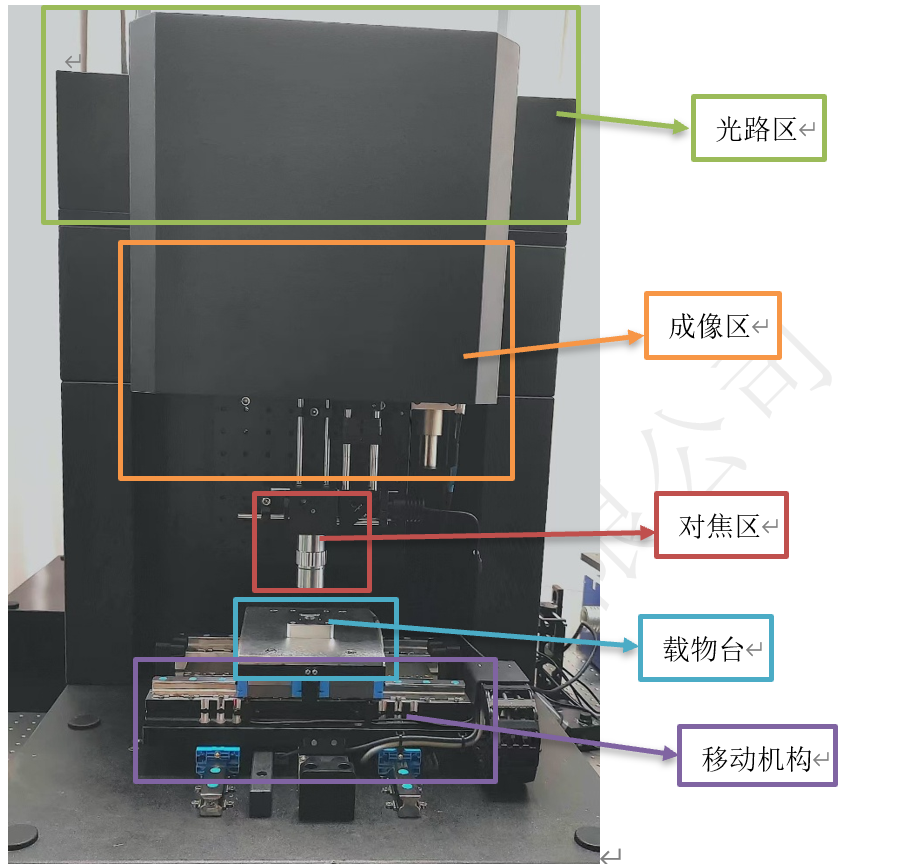
图1 双光子聚合激光直写系统整机结构
2. System Principle
(1) Two-photon polymerization: When femtosecond laser pulses are tightly focused by a high-NA objective, the photon density near the focal point becomes extremely high. Photosensitive materials (photoresist/photosensitive resin) can absorb two photons simultaneously, triggering polymerization. Because the probability of two-photon absorption is proportional to the square of light intensity, the polymerization is strictly confined to an extremely small volume (the “voxel”) near the focus. By precisely moving the focal point, arbitrary 3D structures can be “written” point by point inside the material, with resolution beyond the diffraction limit — the minimum feature size is much smaller than the excitation wavelength.
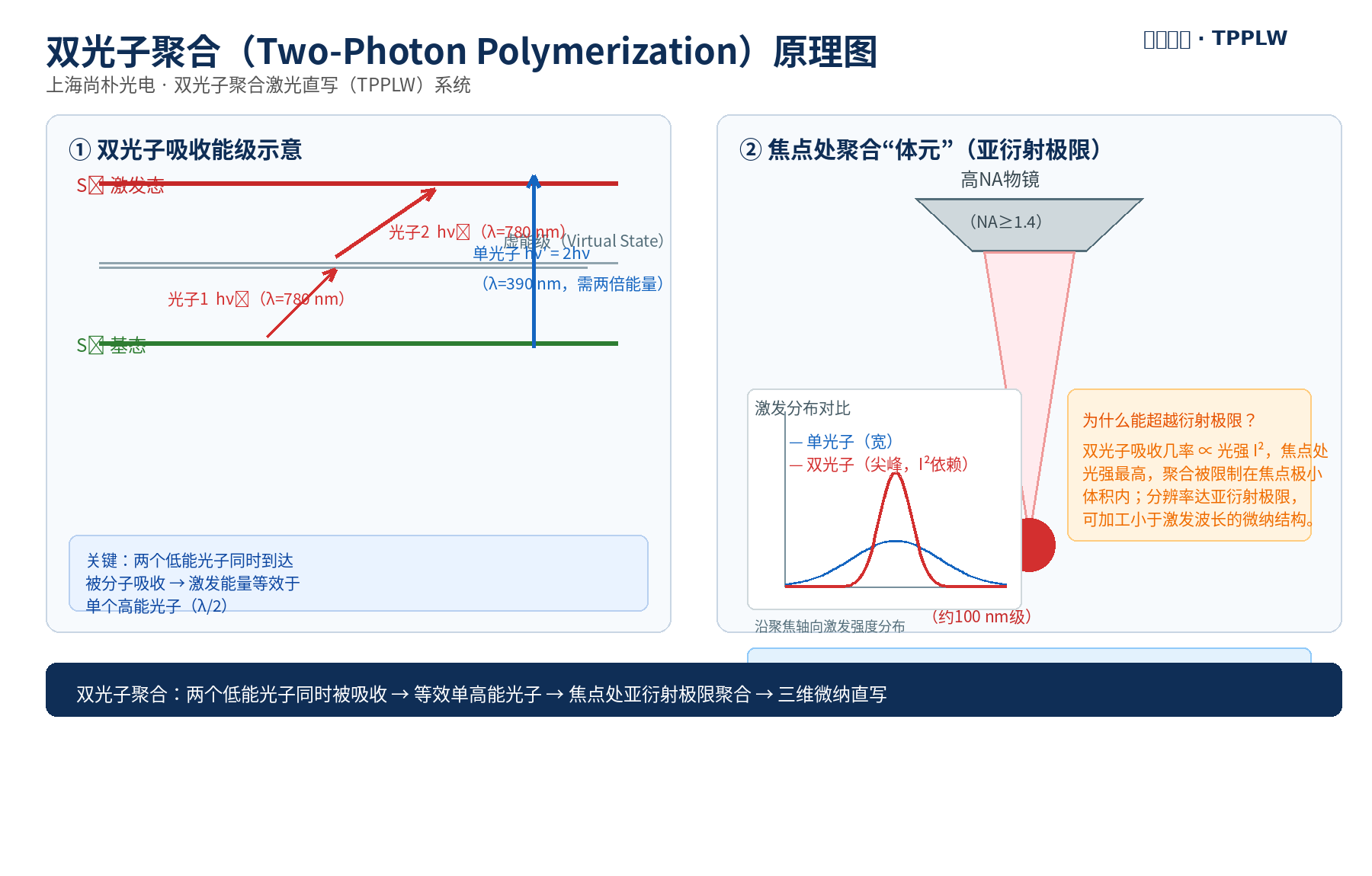
图2 双光子聚合原理图(能级示意与亚衍射极限体元加工)
(2) Optical path: Ultrashort pulses from a fiber femtosecond laser (1560 nm) and second-harmonic generator (SHG, frequency-doubled to 780 nm) pass sequentially through a high-speed optical switch / acousto-optic modulator (AOM, for high-speed on-off control), a pulse compression group (chirped mirror pair / dispersive prism pair for negative GDD compensation), a beam expander group, and a scanning galvanometer (high-speed XY scanning), and are finally tightly focused onto the print material by an immersion high-NA objective. The printing optical path is arranged vertically (parallel to gravity), which suits liquid photosensitive materials and ensures processing stability.
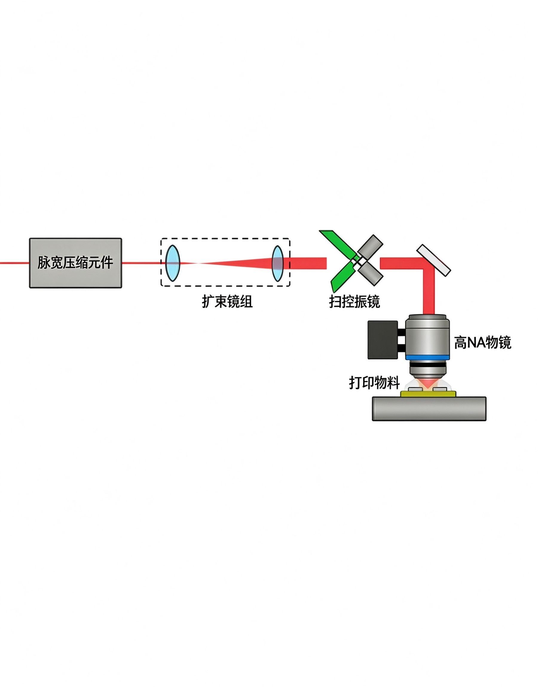
图3 系统光路原理图(光源—高速光开关—脉宽压缩—扩束—扫描振镜—高NA物镜—打印物料)
(3) Microscopy imaging: The system shares the high-NA objective with the printing optical path and integrates a laser confocal scanning microscope, a two-photon fluorescence microscope and a real-time observation system. It supports 3D surface scanning, precise positioning and real-time visual monitoring of metal / semiconductor / glass material interfaces, forming a closed “print-inspect-position” loop.
3. System Composition & Configuration
The system consists of the following functional modules (configurable on request):
- Laser source: 1560 nm fiber femtosecond seed laser + SHG (780±10 nm, pulse width <100 fs, repetition rate ≥80 MHz, average power >140 mW, M²≤1.1); optional 517 nm / 1035 nm dual-wavelength fiber femtosecond laser (4 W) and 671 nm CW laser;
- Pulse compression group: chirped mirror pair (DCM) / dispersive prism pair with continuously tunable negative dispersion (GDD) compensation from -700 to -16000 fs²;
- Focus size control group: immersion high-NA objective (NA≥1.4, oil immersion), tube lens, beam expander (2-8× adjustable), telecentric field lens (f-θ lens);
- Spot position control group: high-precision scanning galvanometer (XY plane) + high-precision voice-coil motor (Z axis), XY position accuracy ≤45 nm, repeatability ≤25 nm;
- Optical on-off control group: mechanical shutter (≥100 Hz) + acousto-optic modulator AOM (modulation rate ≥40 MHz, diffraction efficiency ≥85%);
- Microscopy imaging group: laser confocal scanning microscope (≤480 nm), two-photon fluorescence microscope (450-600 nm), real-time observation system;
- Precision stages: piezoelectric nano stage (2 nm resolution, 300×300×300 μm single scan) or domestic air-bearing 3-axis stage (100×100×10 mm travel, ±0.35 μm accuracy);
- Opto-mechanical platform: high-stability granite platform (grade 00, flatness better than 5 μm), invar / stainless steel opto-mechanical components, multi-DOF fine adjustment mechanisms, sheet-metal stray-light shielding;
- Optional extensions: spatial light modulator (SLM, 1272×1024 pixels, plane multi-focus ≥100, axial multi-focus ≥3), roll-to-roll fiber processing wheels, motorized power attenuator, power meter / polarization state analyzer.
4. Key Specifications
| Parameter | Value |
|---|---|
| Processing wavelength | 780±10 nm (frequency-doubled fs); optional 517 / 1035 nm |
| Laser pulse width | <100 fs (780 nm); <300 fs ~ 10 ps (517 nm) |
| Repetition rate | ≥80 MHz (780 nm); 1 ~ 1 MHz (517 nm) |
| Focused spot | Gaussian spot radius ≤400 nm |
| Minimum line width | ≤30 nm (dual-beam super-resolution); ≤150 nm (single beam) |
| XY positioning / repeatability | ≤45 nm / ≤25 nm |
| Z accuracy / resolution / repeatability | ≤40 nm / ≤20 nm / ≤10 nm |
| Processing field | ≥415 × 348 × 250 μm; optional 300 × 300 × 300 μm |
| Writing speed | ≥1 mm/s (single-point direct writing) |
| Imaging resolution | Confocal ≤480 nm; fluorescence/observation ≤510 nm |
| Environmental requirements | Cleanliness Class-1000; vibration VC-C/VC-E; temperature ±2°C; RH 40-50% |
5. Typical Applications
- Micro-optics: microlens arrays, diffractive optical elements, optical waveguides, photonic crystals, metasurfaces;
- MEMS: micro actuators, micro sensors, micro gears, micro springs;
- Biomedical engineering: 3D cell scaffolds / tissue engineering, microfluidic chips, microneedle arrays, drug delivery structures;
- Optical fiber processing: fiber end-face microstructures, fiber sensors, roll-to-roll continuous fiber direct writing;
- Metamaterials & micro/nano devices: negative-index metamaterials, plasmonic structures, mechanical metamaterials, 3D interconnection structures;
- Materials science: micro/nano direct writing on semiconductors and crystals, 3D processing of multiple materials (metals, semiconductors, glass, perovskites, etc.).
6. Service & Support
Sunpump Opto-Electronic provides full-service support covering requirement analysis, optical system design and simulation, component selection, system integration, installation and commissioning, operator training and after-sales technical support. Configurations can be customized according to processing wavelength, objective magnification, stage travel and processing field size.
1. Overview
The Two-Photon Polymerization Laser Direct Writing (TPPLW) system is based on the two-photon polymerization principle. Femtosecond laser pulses are tightly focused inside a photosensitive material through a high numerical aperture (NA) objective lens, triggering sub-diffraction-limited polymerization at the focal point and building up the print “voxel” point by point. Combined with a high-speed scanning galvanometer and high-precision voice-coil / nano positioning stages for 3D control of the focal spot, the system performs fast, precise fabrication of arbitrary 3D structures within a few hundred micrometers.
Unlike layer-by-layer additive manufacturing, the system fundamentally eliminates the “staircase effect” and produces micro/nano devices with low roughness and high precision. It is widely used in micro-optics, MEMS, biomedical engineering, optical fiber processing and materials science, serving as an ideal platform for advanced precision manufacturing and micro/nano fabrication.
图1 双光子聚合激光直写系统整机结构
2. System Principle
(1) Two-photon polymerization: When femtosecond laser pulses are tightly focused by a high-NA objective, the photon density near the focal point becomes extremely high. Photosensitive materials (photoresist/photosensitive resin) can absorb two photons simultaneously, triggering polymerization. Because the probability of two-photon absorption is proportional to the square of light intensity, the polymerization is strictly confined to an extremely small volume (the “voxel”) near the focus. By precisely moving the focal point, arbitrary 3D structures can be “written” point by point inside the material, with resolution beyond the diffraction limit — the minimum feature size is much smaller than the excitation wavelength.
图2 双光子聚合原理图(能级示意与亚衍射极限体元加工)
(2) Optical path: Ultrashort pulses from a fiber femtosecond laser (1560 nm) and second-harmonic generator (SHG, frequency-doubled to 780 nm) pass sequentially through a high-speed optical switch / acousto-optic modulator (AOM, for high-speed on-off control), a pulse compression group (chirped mirror pair / dispersive prism pair for negative GDD compensation), a beam expander group, and a scanning galvanometer (high-speed XY scanning), and are finally tightly focused onto the print material by an immersion high-NA objective. The printing optical path is arranged vertically (parallel to gravity), which suits liquid photosensitive materials and ensures processing stability.
图3 系统光路原理图(光源—高速光开关—脉宽压缩—扩束—扫描振镜—高NA物镜—打印物料)
(3) Microscopy imaging: The system shares the high-NA objective with the printing optical path and integrates a laser confocal scanning microscope, a two-photon fluorescence microscope and a real-time observation system. It supports 3D surface scanning, precise positioning and real-time visual monitoring of metal / semiconductor / glass material interfaces, forming a closed “print-inspect-position” loop.
3. System Composition & Configuration
The system consists of the following functional modules (configurable on request):
- Laser source: 1560 nm fiber femtosecond seed laser + SHG (780±10 nm, pulse width <100 fs, repetition rate ≥80 MHz, average power >140 mW, M²≤1.1); optional 517 nm / 1035 nm dual-wavelength fiber femtosecond laser (4 W) and 671 nm CW laser;
- Pulse compression group: chirped mirror pair (DCM) / dispersive prism pair with continuously tunable negative dispersion (GDD) compensation from -700 to -16000 fs²;
- Focus size control group: immersion high-NA objective (NA≥1.4, oil immersion), tube lens, beam expander (2-8× adjustable), telecentric field lens (f-θ lens);
- Spot position control group: high-precision scanning galvanometer (XY plane) + high-precision voice-coil motor (Z axis), XY position accuracy ≤45 nm, repeatability ≤25 nm;
- Optical on-off control group: mechanical shutter (≥100 Hz) + acousto-optic modulator AOM (modulation rate ≥40 MHz, diffraction efficiency ≥85%);
- Microscopy imaging group: laser confocal scanning microscope (≤480 nm), two-photon fluorescence microscope (450-600 nm), real-time observation system;
- Precision stages: piezoelectric nano stage (2 nm resolution, 300×300×300 μm single scan) or domestic air-bearing 3-axis stage (100×100×10 mm travel, ±0.35 μm accuracy);
- Opto-mechanical platform: high-stability granite platform (grade 00, flatness better than 5 μm), invar / stainless steel opto-mechanical components, multi-DOF fine adjustment mechanisms, sheet-metal stray-light shielding;
- Optional extensions: spatial light modulator (SLM, 1272×1024 pixels, plane multi-focus ≥100, axial multi-focus ≥3), roll-to-roll fiber processing wheels, motorized power attenuator, power meter / polarization state analyzer.
4. Key Specifications
| Parameter | Value |
|---|---|
| Processing wavelength | 780±10 nm (frequency-doubled fs); optional 517 / 1035 nm |
| Laser pulse width | <100 fs (780 nm); <300 fs ~ 10 ps (517 nm) |
| Repetition rate | ≥80 MHz (780 nm); 1 ~ 1 MHz (517 nm) |
| Focused spot | Gaussian spot radius ≤400 nm |
| Minimum line width | ≤30 nm (dual-beam super-resolution); ≤150 nm (single beam) |
| XY positioning / repeatability | ≤45 nm / ≤25 nm |
| Z accuracy / resolution / repeatability | ≤40 nm / ≤20 nm / ≤10 nm |
| Processing field | ≥415 × 348 × 250 μm; optional 300 × 300 × 300 μm |
| Writing speed | ≥1 mm/s (single-point direct writing) |
| Imaging resolution | Confocal ≤480 nm; fluorescence/observation ≤510 nm |
| Environmental requirements | Cleanliness Class-1000; vibration VC-C/VC-E; temperature ±2°C; RH 40-50% |
5. Typical Applications
- Micro-optics: microlens arrays, diffractive optical elements, optical waveguides, photonic crystals, metasurfaces;
- MEMS: micro actuators, micro sensors, micro gears, micro springs;
- Biomedical engineering: 3D cell scaffolds / tissue engineering, microfluidic chips, microneedle arrays, drug delivery structures;
- Optical fiber processing: fiber end-face microstructures, fiber sensors, roll-to-roll continuous fiber direct writing;
- Metamaterials & micro/nano devices: negative-index metamaterials, plasmonic structures, mechanical metamaterials, 3D interconnection structures;
- Materials science: micro/nano direct writing on semiconductors and crystals, 3D processing of multiple materials (metals, semiconductors, glass, perovskites, etc.).
6. Service & Support
Sunpump Opto-Electronic provides full-service support covering requirement analysis, optical system design and simulation, component selection, system integration, installation and commissioning, operator training and after-sales technical support. Configurations can be customized according to processing wavelength, objective magnification, stage travel and processing field size.
Features
- [{"nameEn": "Two-Photon Polymerization"}, {"nameEn": "Sub-diffraction fabrication"}, {"nameEn": "3D micro-nano direct writing"}]