LBIC
1. Overview The Laser Beam Induced Current Mapping System (LBICS) is an ultra-high-resolution, non-destructive and non-contact imaging analysis system for semic
Products
Sub-categories and products available in this range.
Description
Overview
1. Overview
The Laser Beam Induced Current Mapping System (LBICS) is an ultra-high-resolution, non-destructive and non-contact imaging analysis system for semiconductor optoelectronic devices. By scanning a focused laser beam point-by-point across solar cells, perovskite cells and optoelectronic devices, the system excites localized photovoltaic effects and synchronously records photocurrent signals to construct a two-dimensional photoresponse map. It characterizes short-circuit current distribution, surface defects, shunt resistance and reflectance at the microscale, providing quantitative evidence for structural optimization and process improvement of optoelectronic devices and solar cells.
2. System Principle
LBIC is based on point-by-point scanning of a laser beam over the sample surface. Different wavelengths penetrate to different depths in the semiconductor; photogenerated carriers are separated by the built-in field of the PN junction and form a photocurrent. By acquiring the photocurrent intensity point by point, the carrier collection efficiency, defect density and resistivity distribution are mapped, enabling quantitative characterization of short-circuit current, grain boundaries and dislocations at the microscale.
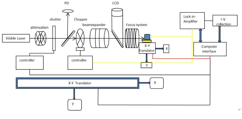
Fig.1 LBIC detection principle
The system supports multi-wavelength combined-beam scanning. Exploiting the wavelength-dependent absorption of different materials, it provides multi-spectral analysis of mainstream photovoltaic materials such as silicon, perovskite and CIGS. A Moire reference grating corrects scanning nonlinearity, keeping geometric image accuracy better than ±1.5 μm.
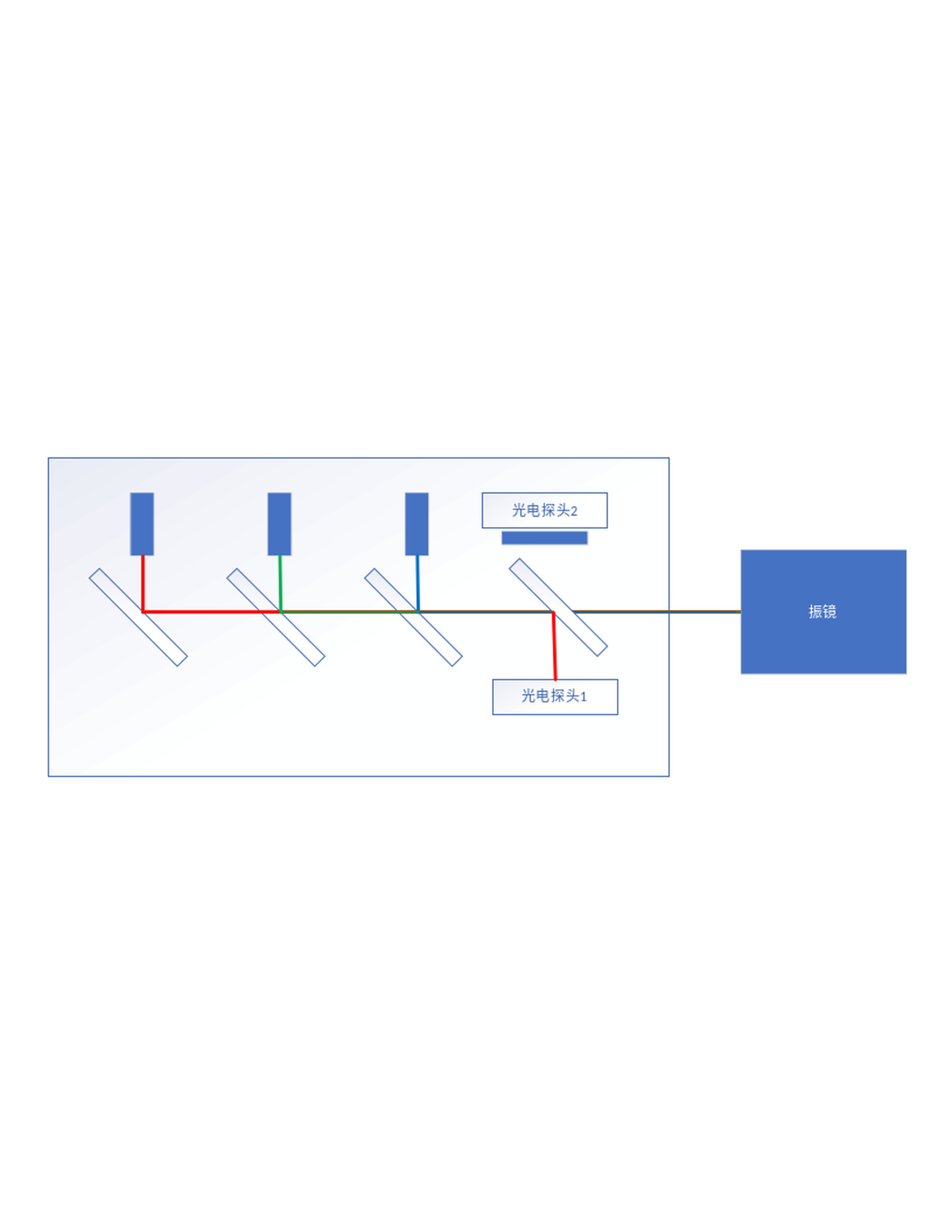
Fig.2 Multi-wavelength beam combining optical path
3. System Composition
The system consists of seven modules:
- Laser source module: multi-wavelength diode lasers (405/455/532/633/650/808 nm optional), programmable power control, stability <±0.5%;
- Beam combining system: dichroic-filter beam combiner merging multiple wavelengths into one path with real-time power monitoring (self-developed);
- High-speed galvanometer scanner: microsecond spot positioning, scan speed up to 8000 points/s, positioning delay <10 μs;
- Precision motion platform: shear lifting stage for Z-axis dynamic focusing, stepper motor with precision rail, positioning accuracy ±2 μm;
- Probe station & sample stage: adapts to different solar cell electrodes with quick sample exchange;
- Signal acquisition module: photodetector for real-time power monitoring, low-noise trans-impedance amplifier (programmable gain), 16-bit multi-channel acquisition card (200 MS/s), channel isolation >80 dB;
- Control & software platform: global-shutter industrial camera for real-time monitoring, laser rangefinder for auto-focusing, LBIC fast scanning software (VB.net/C++ hybrid) for scan-path planning, data modeling and defect recognition.
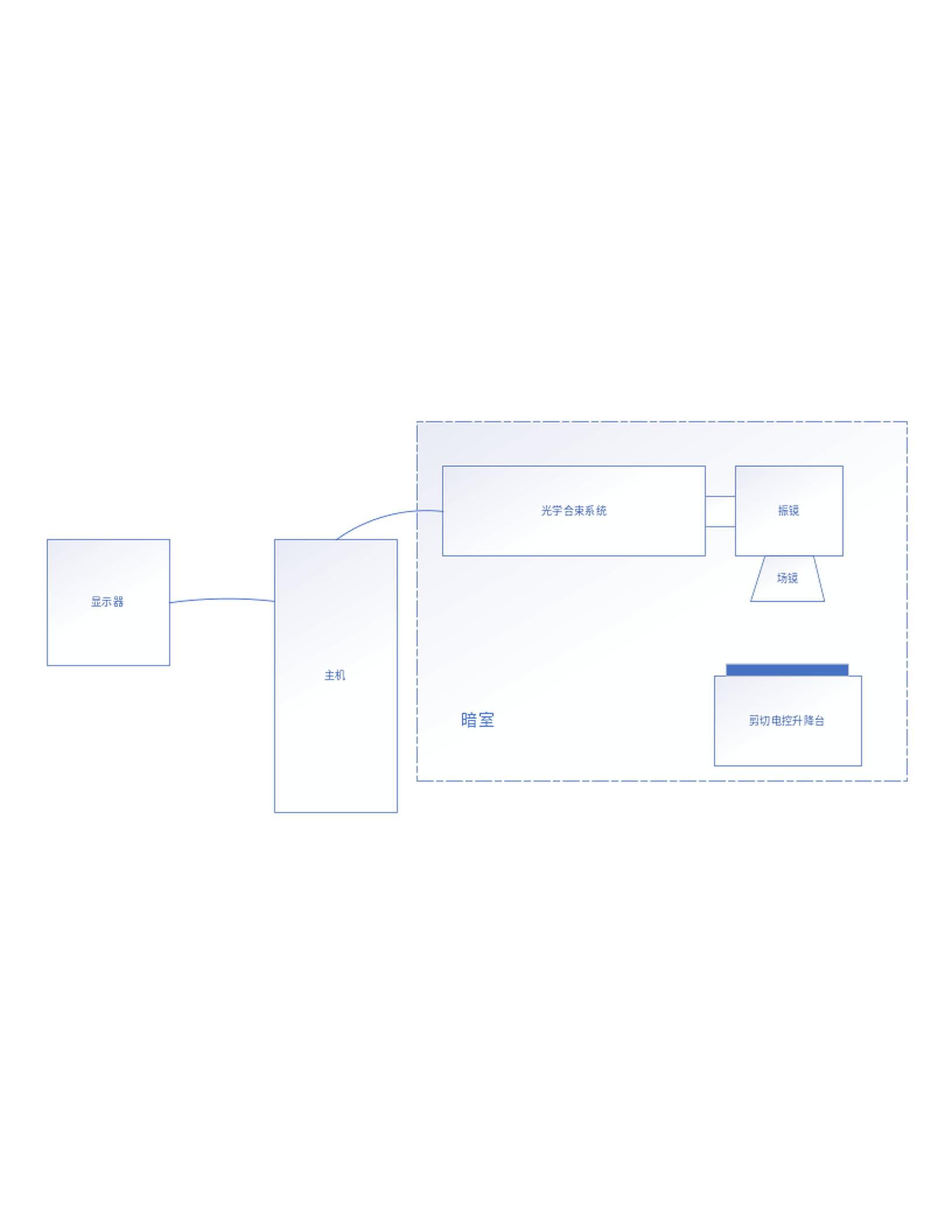
Fig.3 Hardware layout (darkroom design)
4. Key Specifications
| Parameter | Value |
|---|---|
| Excitation wavelengths | 455/532/633/630/808 nm (multi-wavelength optional) |
| Spot diameter | <20 μm (1/e²), stabilized at 15±0.2 μm during scanning |
| Working distance | ≥250 mm |
| Scan speed | 0.5~10 kHz (up to 8000 points/s) |
| Sample positioning accuracy | 5 μm (motion platform ±2 μm) |
| Scan area | 100 mm × 100 mm |
| Power adjustment | 10%~90% |
| Geometric accuracy | better than ±1.5 μm (Moire grating corrected) |
| Signal acquisition | 16-bit, 200 MS/s, channel isolation >80 dB |
| Laser power stability | <±0.5% |
5. Typical Applications
- Solar cell diagnostics: short-circuit current distribution, shunt resistance, surface defects, grain boundary / dislocation imaging;
- Perovskite cell characterization: carrier collection efficiency, uniformity and degraded-region identification;
- Silicon optoelectronic device testing: PN junction quality, carrier lifetime and surface recombination analysis;
- Semiconductor materials research: localized photoresponse, multi-wavelength absorption and quantum efficiency mapping;
- PV production-line QC: high-throughput online inspection and quality control of cells.
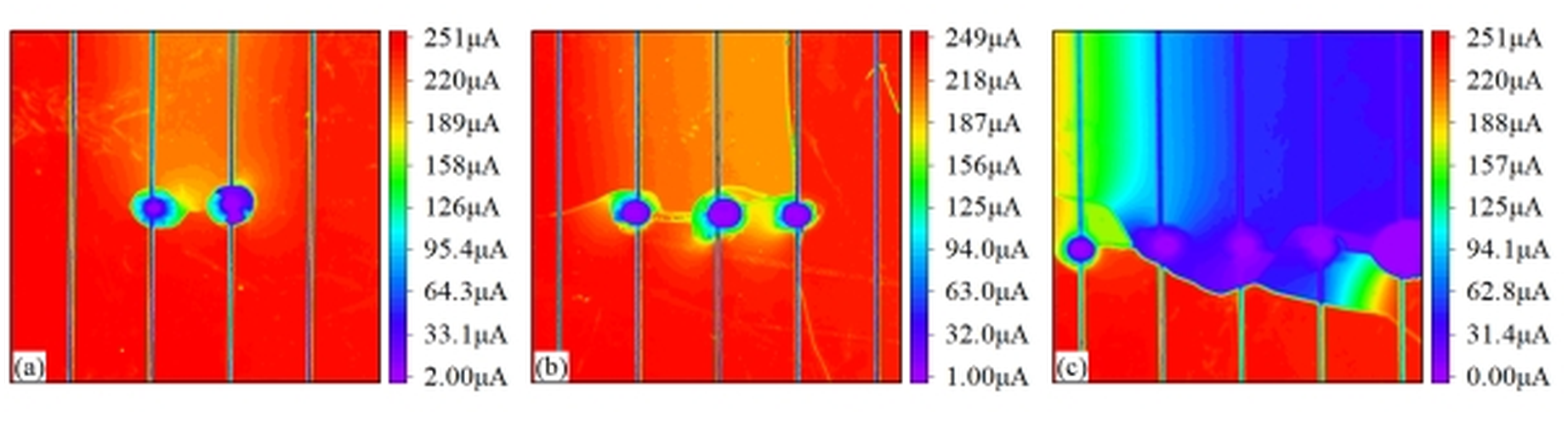
Fig.4 LBIC mapping results of solar cell (current distribution)
6. Software Platform
The LBIC fast scanning software is built on a VB.net/C++ hybrid architecture with multi-threaded pipelining for scan-acquisition-analysis. It supports raster, spiral and custom scan patterns; auto-focusing and scan-path planning; results displayed as color heat maps with structured reports containing defect type, coordinates and confidence; automatic data archiving with traceability, remote diagnostics and OTA upgrades to meet Industry 4.0 data management requirements.
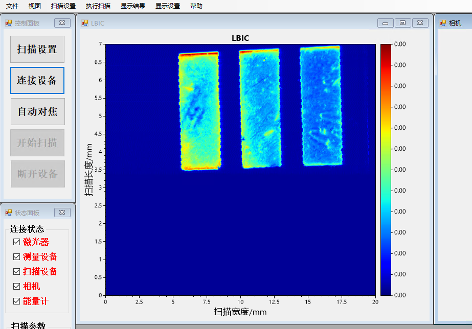
Fig.5 LBIC fast scanning software interface
7. Service & Support
Sunpump Opto-Electronic provides full-service support from requirement analysis, system integration, installation and commissioning to operator training and after-sales service. Wavelengths, scan areas and acquisition channels can be flexibly configured to customer test requirements, with customized solution design available.
1. Overview
The Laser Beam Induced Current Mapping System (LBICS) is an ultra-high-resolution, non-destructive and non-contact imaging analysis system for semiconductor optoelectronic devices. By scanning a focused laser beam point-by-point across solar cells, perovskite cells and optoelectronic devices, the system excites localized photovoltaic effects and synchronously records photocurrent signals to construct a two-dimensional photoresponse map. It characterizes short-circuit current distribution, surface defects, shunt resistance and reflectance at the microscale, providing quantitative evidence for structural optimization and process improvement of optoelectronic devices and solar cells.
2. System Principle
LBIC is based on point-by-point scanning of a laser beam over the sample surface. Different wavelengths penetrate to different depths in the semiconductor; photogenerated carriers are separated by the built-in field of the PN junction and form a photocurrent. By acquiring the photocurrent intensity point by point, the carrier collection efficiency, defect density and resistivity distribution are mapped, enabling quantitative characterization of short-circuit current, grain boundaries and dislocations at the microscale.
Fig.1 LBIC detection principle
The system supports multi-wavelength combined-beam scanning. Exploiting the wavelength-dependent absorption of different materials, it provides multi-spectral analysis of mainstream photovoltaic materials such as silicon, perovskite and CIGS. A Moire reference grating corrects scanning nonlinearity, keeping geometric image accuracy better than ±1.5 μm.
Fig.2 Multi-wavelength beam combining optical path
3. System Composition
The system consists of seven modules:
- Laser source module: multi-wavelength diode lasers (405/455/532/633/650/808 nm optional), programmable power control, stability <±0.5%;
- Beam combining system: dichroic-filter beam combiner merging multiple wavelengths into one path with real-time power monitoring (self-developed);
- High-speed galvanometer scanner: microsecond spot positioning, scan speed up to 8000 points/s, positioning delay <10 μs;
- Precision motion platform: shear lifting stage for Z-axis dynamic focusing, stepper motor with precision rail, positioning accuracy ±2 μm;
- Probe station & sample stage: adapts to different solar cell electrodes with quick sample exchange;
- Signal acquisition module: photodetector for real-time power monitoring, low-noise trans-impedance amplifier (programmable gain), 16-bit multi-channel acquisition card (200 MS/s), channel isolation >80 dB;
- Control & software platform: global-shutter industrial camera for real-time monitoring, laser rangefinder for auto-focusing, LBIC fast scanning software (VB.net/C++ hybrid) for scan-path planning, data modeling and defect recognition.
Fig.3 Hardware layout (darkroom design)
4. Key Specifications
| Parameter | Value |
|---|---|
| Excitation wavelengths | 455/532/633/630/808 nm (multi-wavelength optional) |
| Spot diameter | <20 μm (1/e²), stabilized at 15±0.2 μm during scanning |
| Working distance | ≥250 mm |
| Scan speed | 0.5~10 kHz (up to 8000 points/s) |
| Sample positioning accuracy | 5 μm (motion platform ±2 μm) |
| Scan area | 100 mm × 100 mm |
| Power adjustment | 10%~90% |
| Geometric accuracy | better than ±1.5 μm (Moire grating corrected) |
| Signal acquisition | 16-bit, 200 MS/s, channel isolation >80 dB |
| Laser power stability | <±0.5% |
5. Typical Applications
- Solar cell diagnostics: short-circuit current distribution, shunt resistance, surface defects, grain boundary / dislocation imaging;
- Perovskite cell characterization: carrier collection efficiency, uniformity and degraded-region identification;
- Silicon optoelectronic device testing: PN junction quality, carrier lifetime and surface recombination analysis;
- Semiconductor materials research: localized photoresponse, multi-wavelength absorption and quantum efficiency mapping;
- PV production-line QC: high-throughput online inspection and quality control of cells.
Fig.4 LBIC mapping results of solar cell (current distribution)
6. Software Platform
The LBIC fast scanning software is built on a VB.net/C++ hybrid architecture with multi-threaded pipelining for scan-acquisition-analysis. It supports raster, spiral and custom scan patterns; auto-focusing and scan-path planning; results displayed as color heat maps with structured reports containing defect type, coordinates and confidence; automatic data archiving with traceability, remote diagnostics and OTA upgrades to meet Industry 4.0 data management requirements.
Fig.5 LBIC fast scanning software interface
7. Service & Support
Sunpump Opto-Electronic provides full-service support from requirement analysis, system integration, installation and commissioning to operator training and after-sales service. Wavelengths, scan areas and acquisition channels can be flexibly configured to customer test requirements, with customized solution design available.
Features
- [{"nameEn": "Multi-wavelength scanning"}, {"nameEn": "High-speed galvanometer scanning"}, {"nameEn": "Non-destructive imaging"}]