Light-Beam Induced Current
Overview
The Multi-Wavelength High-Speed LBIC Detection System (H-LBIC-1000) addresses the high-throughput inspection demand of optoelectronic devices, solar cells and perovskite cells, breaking the bottleneck of slow scan speed in conventional LBIC. High-speed galvanometer scanning, time synchronization and wavelet algorithm optimization enable rapid high-quality imaging; multi-wavelength switching at 455/532/630/808 nm covers silicon, perovskite and CIGS photovoltaic materials, with scan speeds up to 5 kHz.
Description
1. Overview
The H-LBIC-1000 Multi-Wavelength High-Speed Laser Beam Induced Current Detection System is a new-generation high-speed LBIC inspection platform for characterization and defect detection of semiconductor optoelectronic devices, solar cells and perovskite cells. It breaks the bottleneck of slow scan speed and long acquisition time of conventional LBIC, has been applied at Sunpump with ideal results, and reaches an advanced domestic level.
2. Detection Principle
The system is based on point-by-point scanning of the laser beam over the cell surface, exciting localized photovoltaic effects to obtain current response signals. Multi-wavelength sources combined with the absorption characteristics of different materials enable comprehensive analysis of PN junction quality, carrier lifetime and surface recombination rate. High-precision galvanometer scanning and dynamic focusing position the laser spot at the micron scale; photocurrent intensity at each point is synchronously recorded to build a two-dimensional photoresponse map. Machine vision locates defect position and morphology; edge-enhancement algorithms extract low-contrast defect features; spatial-frequency filtering suppresses ambient noise; a Moire reference grating corrects scanning nonlinearity, keeping geometric image accuracy better than ±1.5 μm.
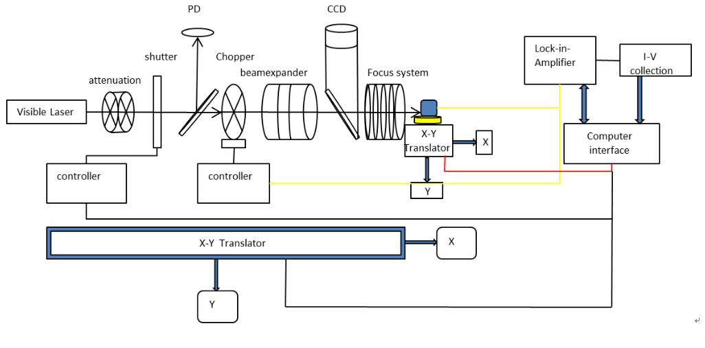
Fig.1 LBIC detection principle
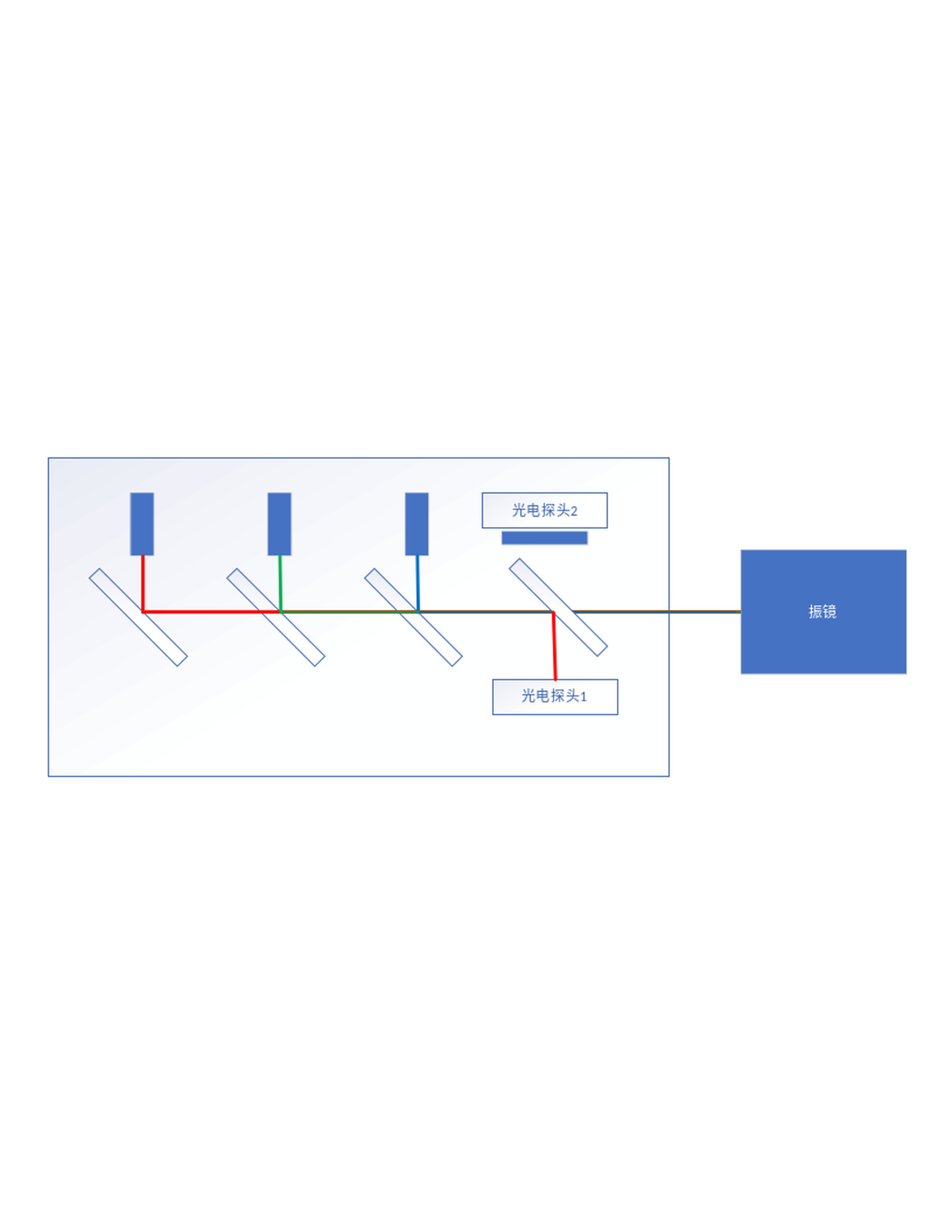
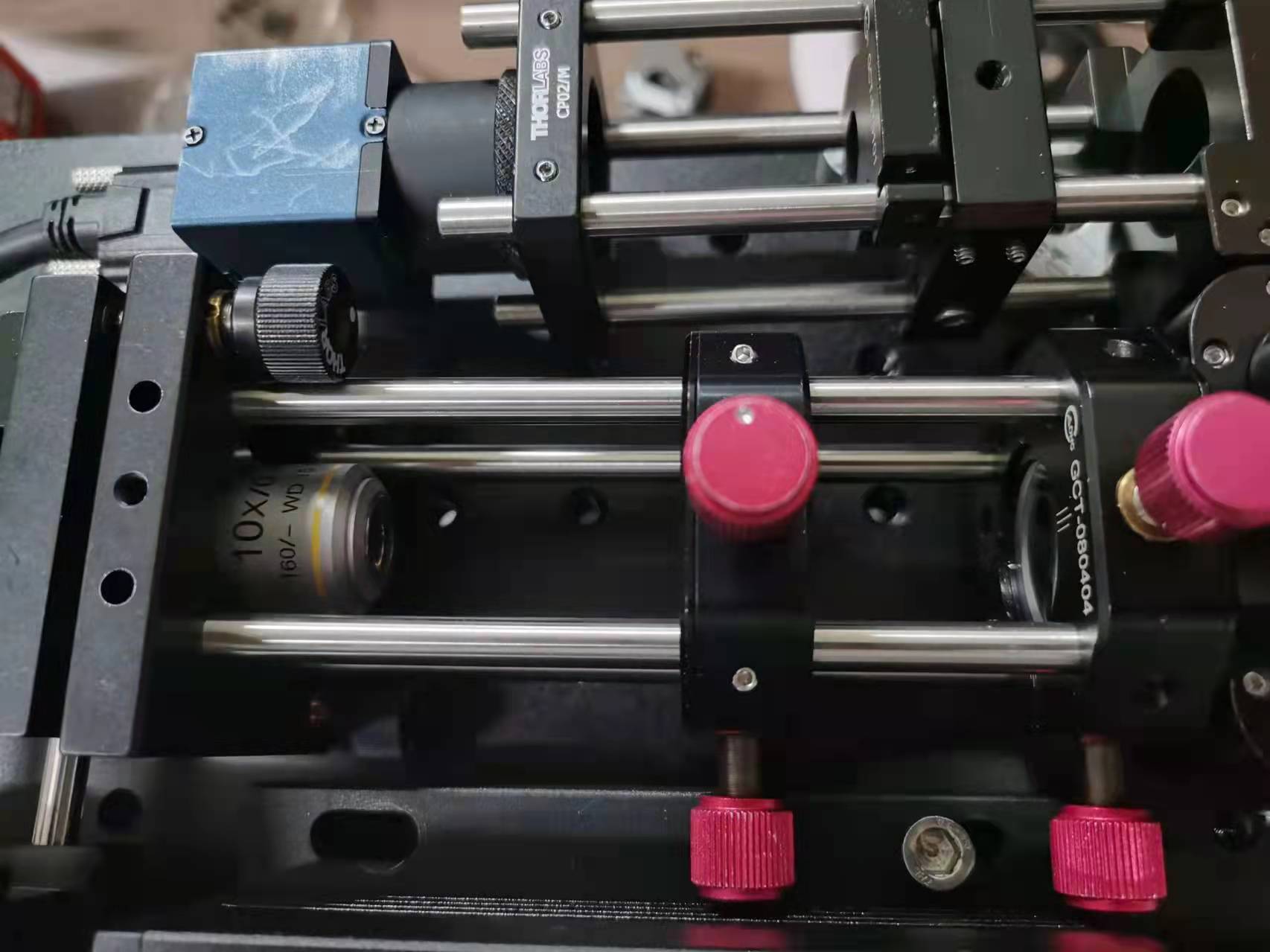
Fig.2 Multi-wavelength beam combining optical path
3. Four Technical Innovations
- High-speed galvanometer scanning: rapid inspection of optoelectronic devices at up to 5 kHz scan speed;
- High-speed time synchronization: hardware-triggered synchronization between galvanometer control and acquisition card ensures each sampling point strictly corresponds to the laser position, solving high-speed positioning;
- Wavelet algorithm optimization: high-quality imaging and defect feature identification;
- Multi-wavelength switching: 455/532/630/808 nm integrated, relay auto-switching by software, adapting to different material absorption.
4. System Composition
- Laser source module: multi-wavelength diode lasers (455/532/630/808 nm), constant-current driving, power fluctuation <±0.5%;
- Beam combining system: multi-wavelength combination with real-time power monitoring;
- High-speed galvanometer scanner: 8000 points/s, positioning delay <10 μs, raster / spiral / custom trajectories;
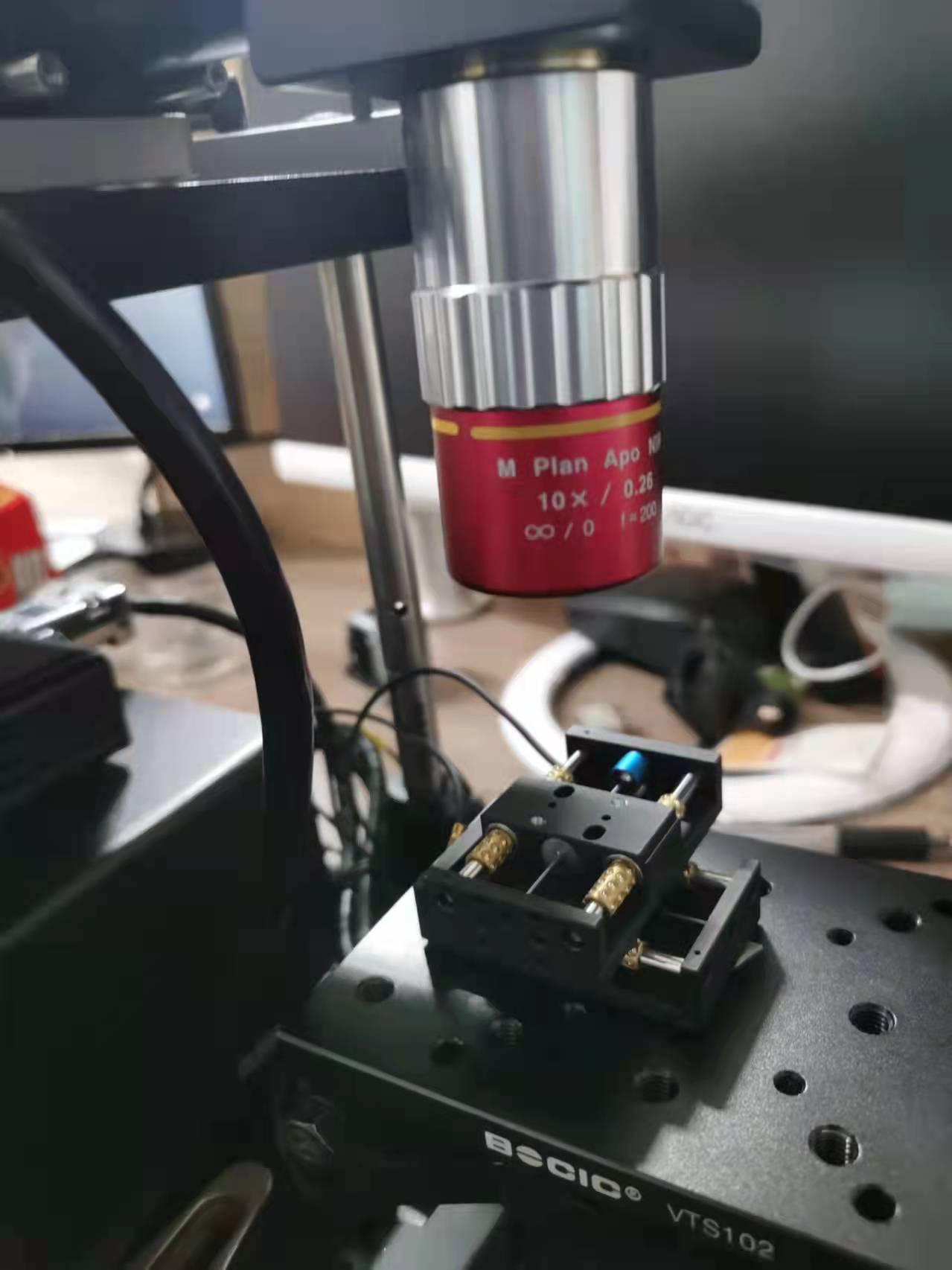
- Precision motion platform: shear lifting stage for Z-axis dynamic focusing, 256-subdivision stepper, positioning accuracy ±2 μm;
- Probe station & sample stage: quick sample exchange with reliable contact;
- Signal acquisition module: low-noise trans-impedance amplifier (programmable gain), 16-bit multi-channel card at 200 MS/s, channel isolation >80 dB;
- Control & software platform: global-shutter industrial camera, laser rangefinder auto-focusing, LBIC fast scanning software for scan-acquisition-analysis pipelining.
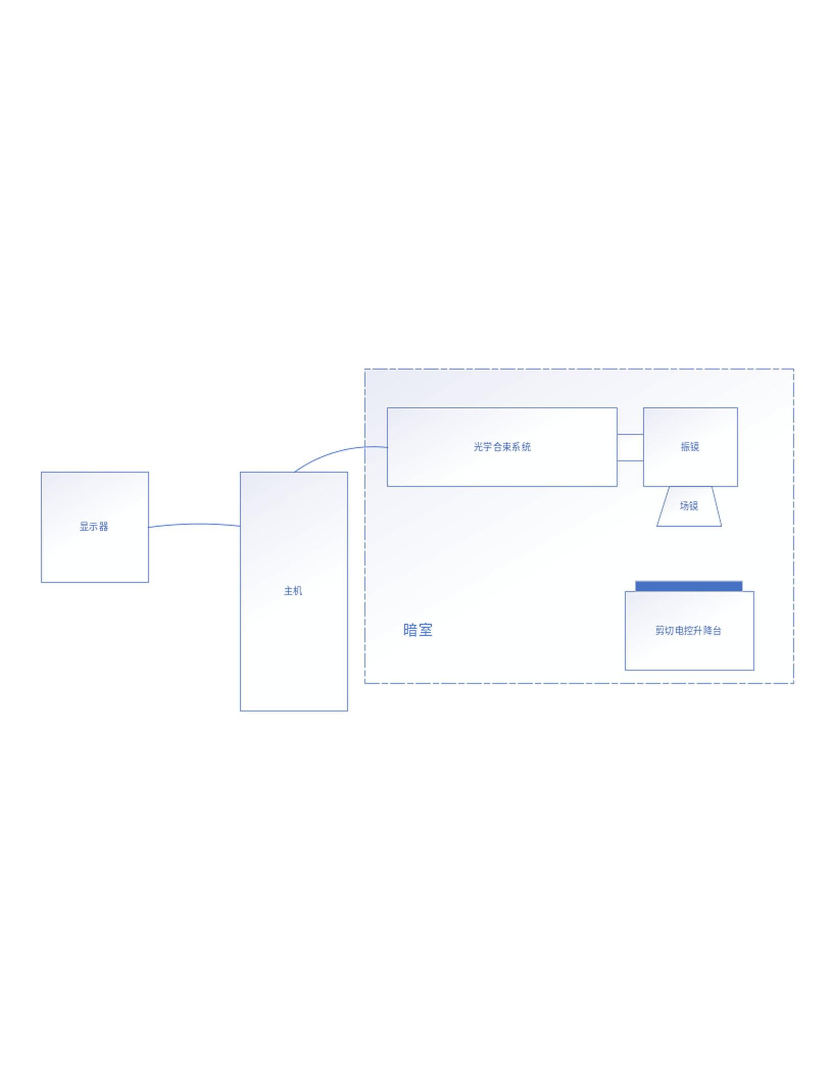
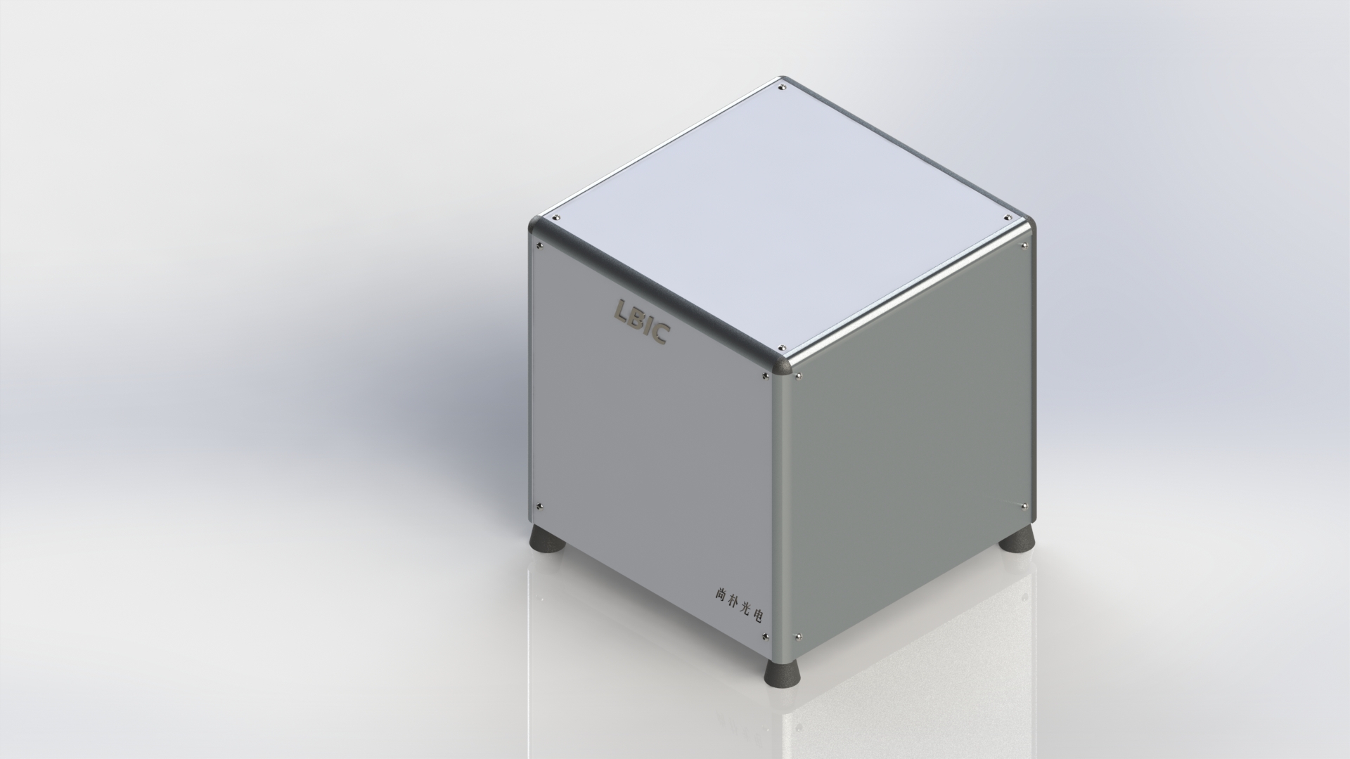
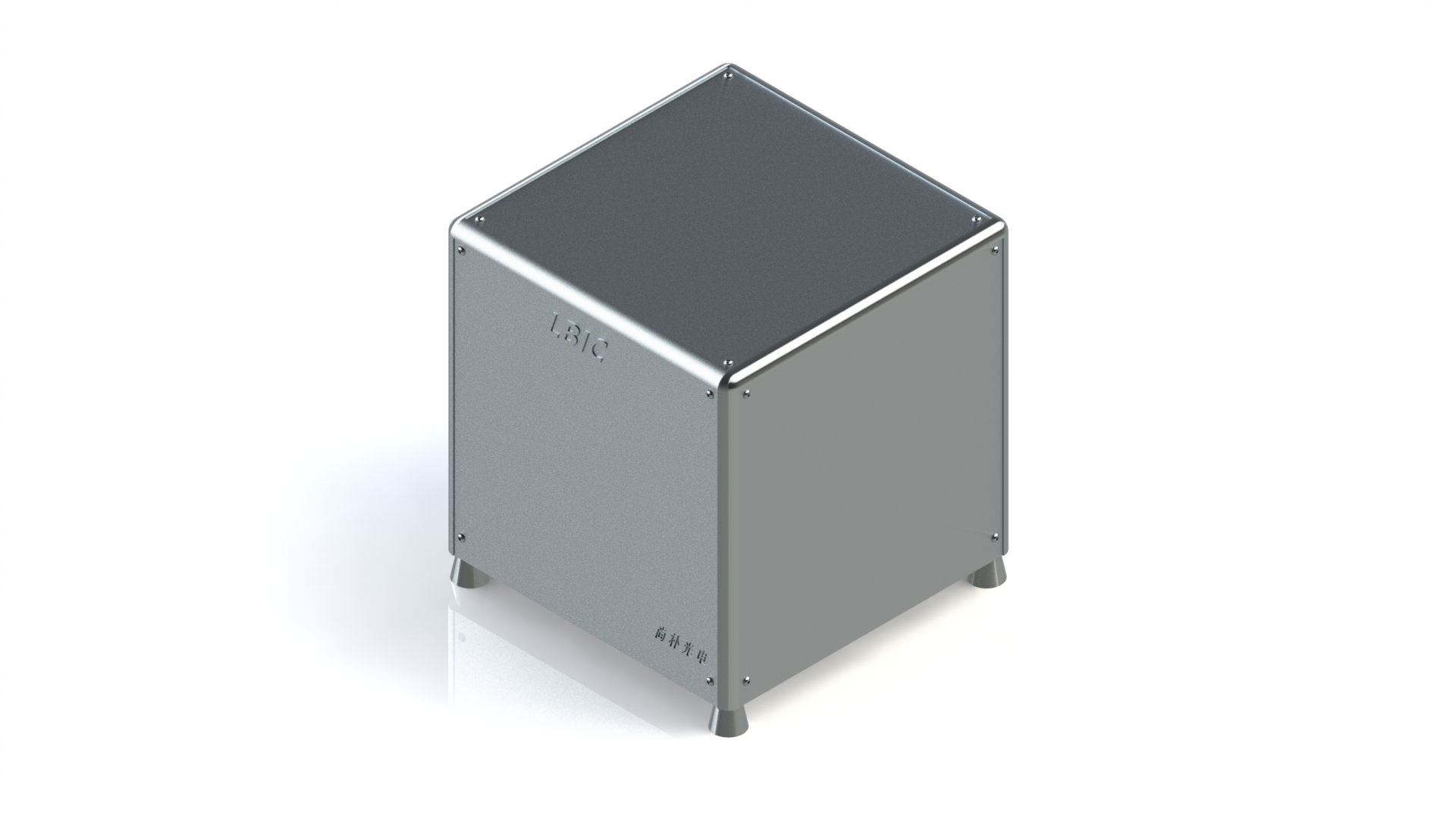
Fig.3 Hardware layout (darkroom design)
5. Key Specifications
| Parameter | Value |
|---|---|
| Excitation wavelengths | 455/532/630/808 nm integrated |
| Spot diameter | <20 μm (1/e²), stabilized at 15±0.2 μm |
| Working distance | ≥250 mm |
| Sample positioning accuracy | 5 μm |
| Power adjustment | 10%~90% |
| Scan area | 100 mm × 100 mm |
| Scan speed | 5 kHz (up to 8000 points/s) |
| Geometric accuracy | better than ±1.5 μm |
| Signal acquisition | 16-bit, 200 MS/s, channel isolation >80 dB |
6. Software Platform
The LBIC fast scanning software supports scan settings, device connection, auto-focus, scan mode / range / speed / steps / laser power configuration; results are shown as color heat maps with structured reports containing defect type, coordinates and confidence, meeting high-throughput online inspection needs of PV production lines.
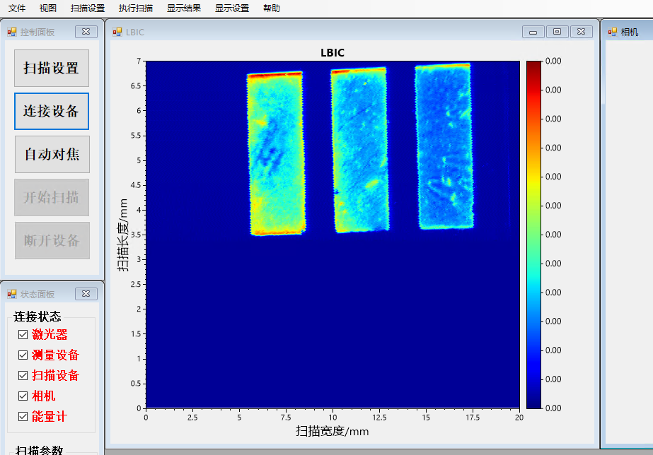
Fig.4 LBIC fast scanning software interface
7. Typical Applications
- Solar cell short-circuit current distribution, shunt resistance, surface defects and grain boundary / dislocation imaging;
- Perovskite cell carrier collection efficiency, uniformity and degraded-region identification;
- Silicon device PN junction quality and carrier lifetime analysis;
- Multi-wavelength absorption and quantum efficiency mapping of semiconductor materials;
- High-throughput online inspection and quality control of PV production lines.
8. Service & Support
Sunpump provides full-service support from requirement analysis, system integration, installation and commissioning to training and after-sales service, with flexible configuration.
Specifications
| wavelength | 532nm,633nm,785nm |
| 分辨率 | 2um-100um |
| 检测速度 | 0.5-10KHZ |
Technical Data