Light-Beam Induced Current
Overview
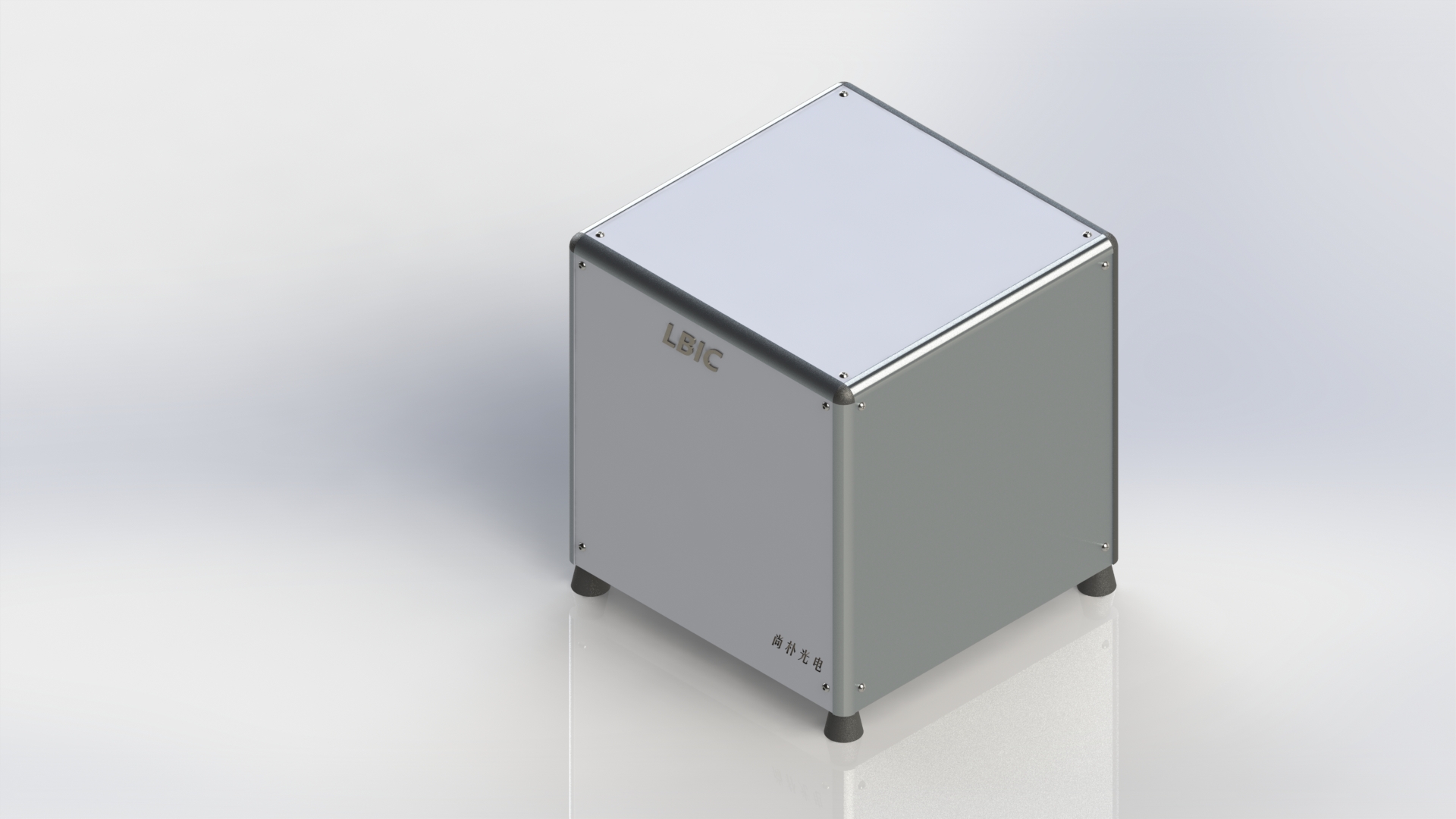
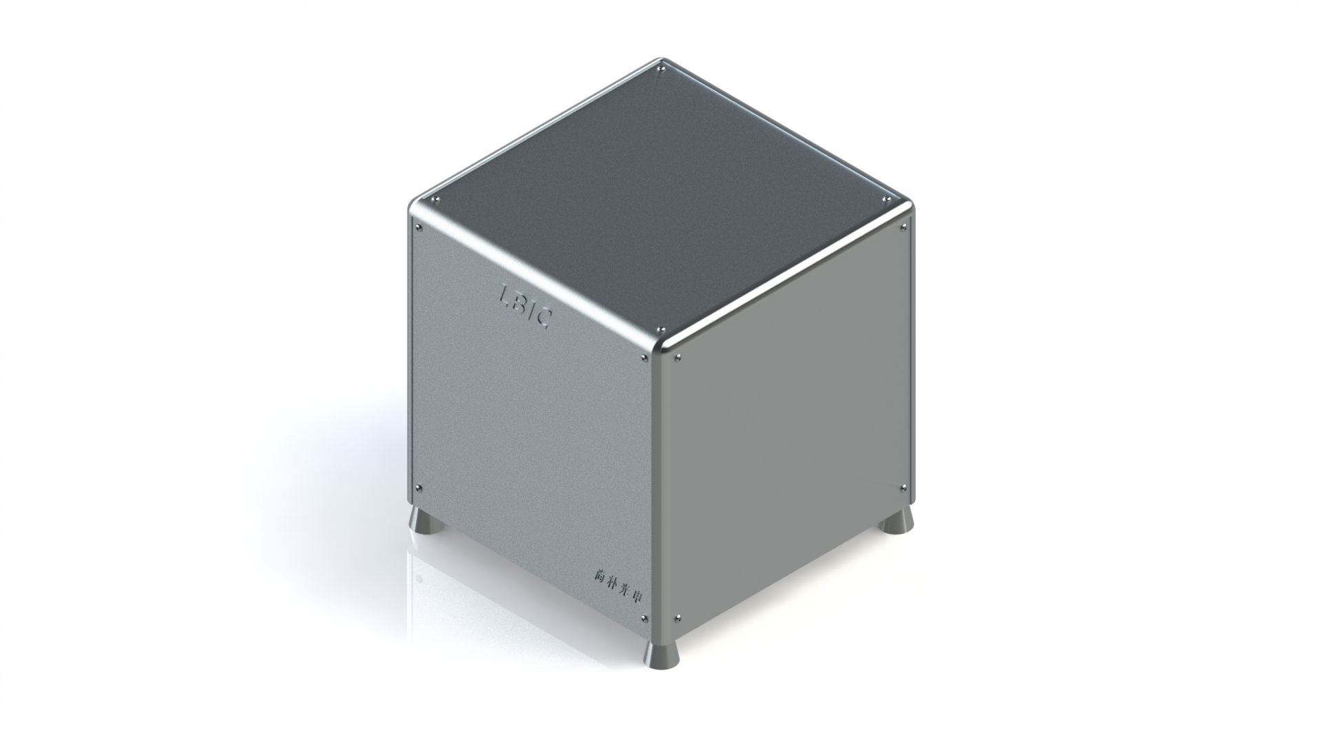
The Laser Beam Induced Current Detection System (LBIC-1000) scans a focused laser beam point-by-point across solar cells, perovskite cells and semiconductor optoelectronic devices. By synchronously acquiring photocurrent signals from localized photovoltaic effects, it constructs two-dimensional photoresponse maps for non-destructive, non-contact characterization of short-circuit current distribution, surface defects, shunt resistance, grain boundaries and dislocations, providing reliable evidence for structural optimization and process improvement.
Description
1. Overview
The LBIC-1000 Laser Beam Induced Current Detection System is an ultra-high-resolution, non-destructive and non-contact imaging analysis system for solar cells, silicon photocells, perovskite cells and semiconductor optoelectronic devices.
2. Detection Principle
Different laser wavelengths penetrate to different depths in semiconductors. Photogenerated carriers produced by the focused laser spot are separated by the built-in field of the PN junction and form a photocurrent. By scanning point by point and acquiring the photocurrent intensity, the system maps carrier collection efficiency, defect density and resistivity distribution, enabling quantitative characterization of short-circuit current, grain boundaries and dislocations; lateral scanning (mapping) imaging reflects the planar uniformity of device parameters.
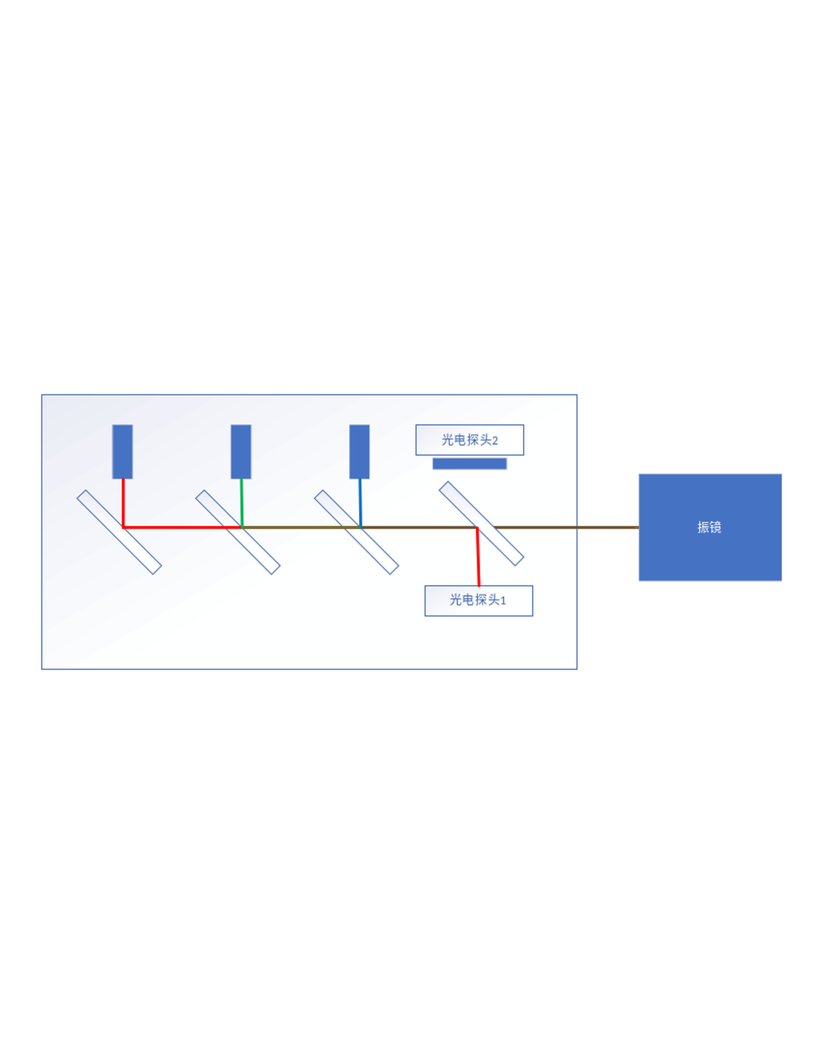
Fig.1 Multi-wavelength beam combining optical path
3. System Composition
- Laser source module: multi-wavelength diode lasers (532/633/785 nm), adjustable power;
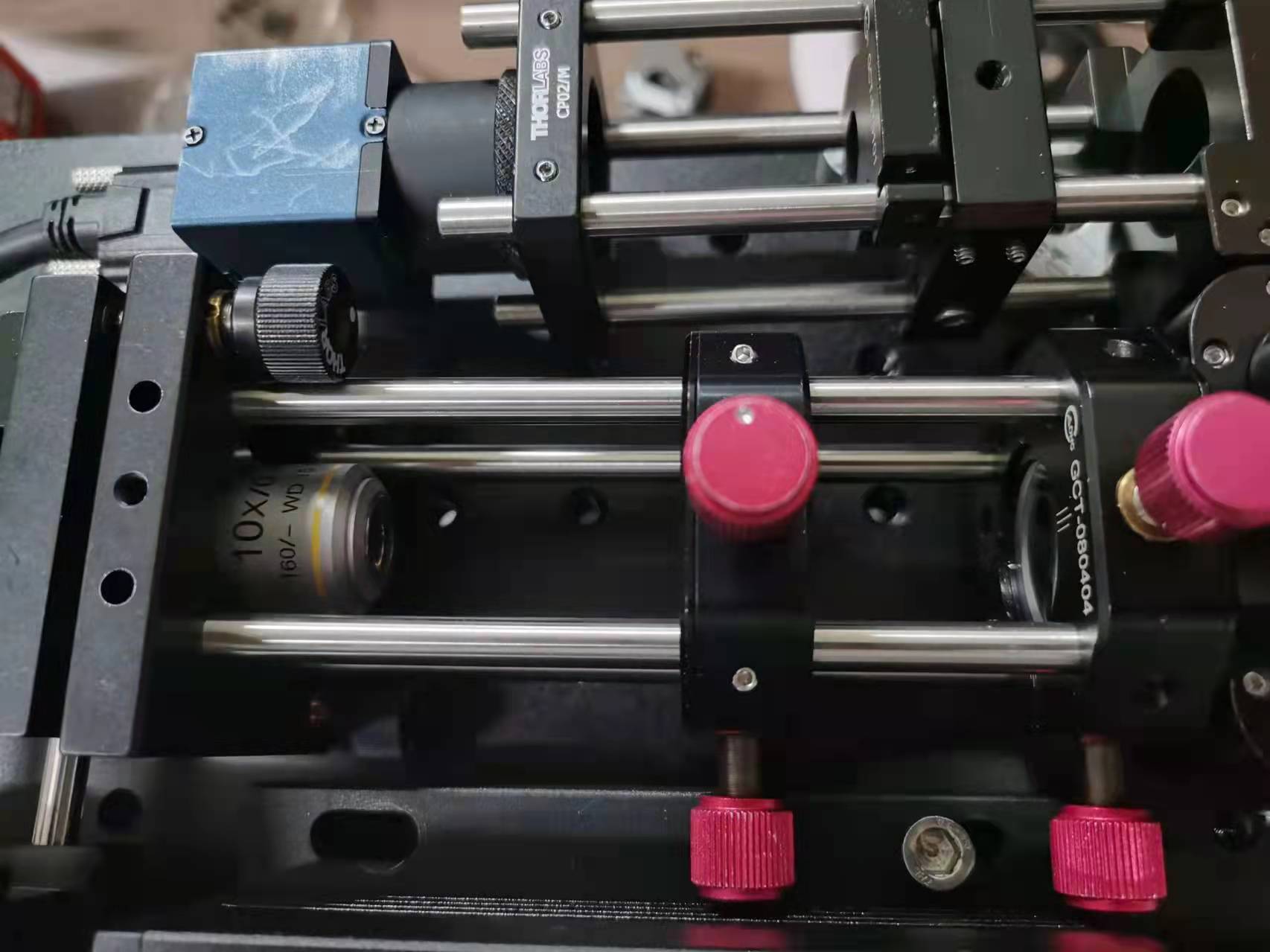
- Beam combining system: multi-wavelength combination with real-time photodetector power monitoring;
- High-speed galvanometer scanner: microsecond spot positioning, raster / spiral / custom scan patterns;
- Precision motion platform: Z-axis dynamic focusing, stepper-motor driven, high positioning accuracy;
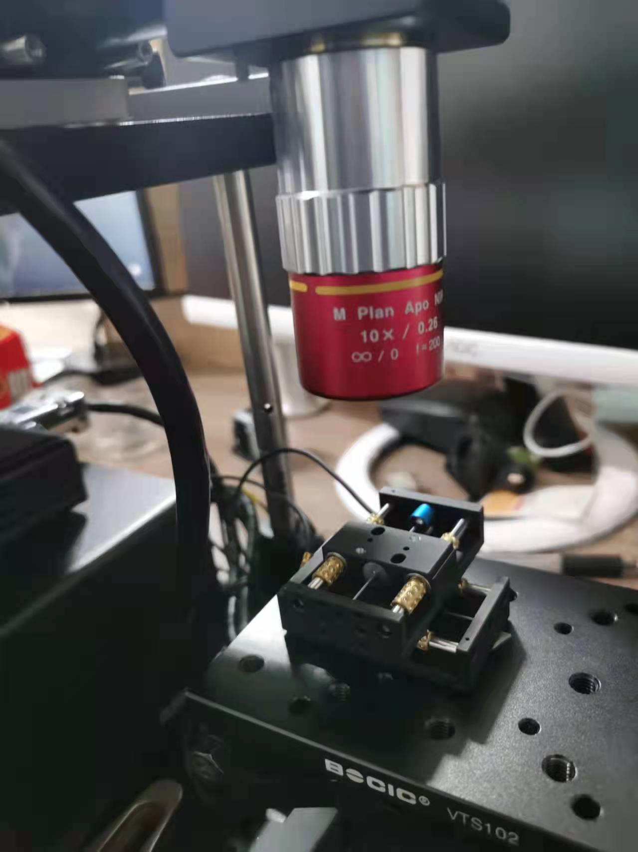
- Probe station & sample stage: adapts to different cell electrodes with quick sample exchange;
- Signal acquisition module: low-noise trans-impedance amplifier, 16-bit multi-channel acquisition card;
- Control & software platform: LBIC fast scanning software for scan-path planning, data modeling and defect recognition.
4. Features
- Ultra-high-resolution, non-destructive, non-contact imaging inspection;
- Multi-wavelength scanning compatible with silicon, perovskite and other mainstream PV materials;
- High-precision galvanometer cooperative control with micron-level positioning accuracy;
- Machine vision integrated with laser intensity detection for surface defect recognition and photoresponse mapping;
- Custom software platform for automated workflows and visualized results, greatly improving throughput.
5. Typical Applications
- Solar cell short-circuit current distribution, shunt resistance and surface defect detection;
- Perovskite cell carrier collection efficiency and uniformity characterization;
- Silicon device PN junction quality, carrier lifetime and surface recombination analysis;
- Semiconductor microscale photoresponse and quantum efficiency mapping;
- High-throughput PV production-line cell quality inspection.
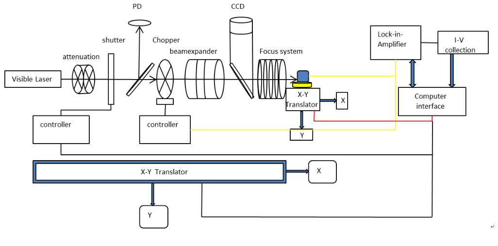
Fig.2 LBIC detection principle
6. Service & Support
Sunpump provides full-service support covering requirement analysis, system integration, installation and commissioning, operator training and after-sales service, with flexible configuration to customer test requirements.
Specifications
| wavelength | 532nm,633nm,785nm |
| 分辨率 | 2um-100um |
| 检测速度 | 0.5-10KHZ |
Technical Data